High Voltage and X-Ray Experiments
Text and Graphics Copyright © 2005 − 2008 Henning Umland
The following descriptions are given for the purpose of information only. I do not encourage ANYBODY to conduct experiments like those shown below, and I do not assume liability for any damage resulting from such experiments. People working with high voltage and X-rays should have a solid background in physics and electronics and should know what they are doing. The high voltage sources described here are much more powerful than generators of static electricity like, e. g., influence machines, Van de Graaff generators, etc. High voltage can kill instantly, X-rays in the long run (radiation sickness, cancer) if not handled properly.
Experiments with Various Multiplier Designs (I)
The following experiments were made to compare the output impedance of various voltage multipliers differing in design and stage number. The components used for the circuits were 3 A silicon diodes and oil/paper capacitors (C = 20 μF ± 5%). Up to three identical 80 W power transformers were used as AC voltage sources (approx. 43 V RMS).
Although I made these measurements with greatest care, the numbers obtained are only moderately accurate. This is due to the fact that a transformer is not an ideal AC source but has a certain output impedance caused by wire resistance and leak inductance. The output impedance of the transformer is not quite negligible because a multiplier running under load draws high peak currents (like any rectifier circuit with a load capacitor). Capacitors and diodes, too, are real-world, lossy components. All of these factors affect the output impedance of a multiplier. Moreover, the differential output impedance, dU/dI, is a function of the load current (decreasing as the load current increases). To keep the resulting error as small as possible, I applied only light to moderate loads (keeping the voltage drop, ΔU, below 20%). Last but not least, I had to struggle with rapid fluctuations of the 230 V line voltage which made it difficult to obtain highly accurate ΔU values. To reduce the error, I made multiple measurements and took the median of 5 values every time. Although the experimental error may reach ±10%, the tabulated numbers may be helpful when designing a multiplier for a given application.
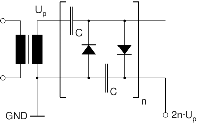
The first diagram shows a single-phase (half-wave) voltage multiplier consisting of an array of n doubler stages. All capacitances in the circuit are equal. The circuit consists of two series stacks of capacitors, the "charging stack" (on top) and the "load stack" (the one connected to the output terminal). Both are interconnected by a meandering stack of diodes. The output voltage (open circuit) is an even multiple of the AC peak voltage supplied by the transformer (neglecting the forward voltage of the diodes). The AC peak voltage supplied by the transformer, Up, is √2·URMS, provided the sine wave is not distorted. The disadvantage of the single-phase multiplier is that the load stack not only has to store the electrical charge which flows through the load resistor (not shown in the diagram) and smoothe the output voltage but also has to recharge the charging stack during the negative half wave. This results in comparatively bad voltage regulation and high ripple voltage under load.
|
Circuit Diagram of Single-Phase (Half-Wave) Multiplier with n doubler stages (classical Cockcroft-Walton Circuit)
The problems associated with the single phase multiplier are largely overcome by the 2-phase (full-wave) design. One can imagine this as a back-to-back arrangement of two half-wave multipliers sharing one load stack. The AC input voltages have to be 180° out of phase (push-pull mode) which can be achieved through two identical transformers or through a single transformer with a center tap in the secondary coil. Here, the two charging stacks recharge each other alternatingly (at the same time recharging the load stack) while the load stack itself mainly serves as a low-pass filter reducing the ripple voltage under load. A 2-phase multiplier can also be imagined as a series stack of full-wave rectifier bridges fed by two series stacks of capacitors. The load stack can be omitted and replaced with a single load capacitor (with higher voltage rating) across the output terminals. The circuit is particularly suitable for transformers with a grounded secondary coil (one output terminal connected to the iron core). For example, many microwave oven transformers and oil burner ignition transformers are built this way to avoid thick coil insulations.
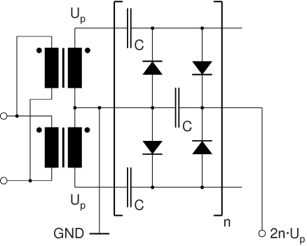 |
Circuit Diagram of 2-Phase (Full-Wave) Multiplier with Grounded Transformer Coils
The full-wave multiplier is a special case of a polyphase multiplier in which several multipliers share a common stack of load capacitors. The circuit diagram of a three-phase multiplier is shown below. Again, the peak voltage supplied by each secondary coil is UP. In this case, the phase angle is 0°, 120°, and 240°, respectively.
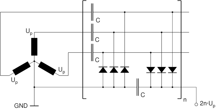 |
Circuit Diagram of 3-Phase Multiplier (Y Configuration with Grounded Center Point)
The following is a summary of my experimental results obtained with the designs described above. I did not go beyond 5 stages since multipliers of higher order are not suitable for my applications (bad voltage regulation). The output voltages were measured with a 10 MΩ digital voltmeter (Amprobe 37XR-A). To measure the average voltage, a low-pass filter consisting of a 100 kΩ resistor and a 2.5 μF oil/paper capacitor (0.25 s time constant) was used to suppress the AC components (ripple) occuring under load. Because of the 100 kΩ resistor, the DC voltages indicated by the instrument are 1% too low, but this is cancelled out when calculating the output impedance (the calculated load current is also 1% too low).
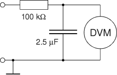 |
Digital Voltmeter with Low-Pass Filter
The measurements were made as follows. First, the no-load voltage, U0, is measured. The voltage measurement is repeated after connecting a load resistor, RL, to the output terminals of the multiplier. Thus, the voltage under load, UL, is obtained. UL/RL is the load current, IL. U0-UL is the voltage drop under load, ΔU. The quotient ΔU/IL is the (approximate) output impedance of the circuit, Zi. Zi is proportional to the reactance of C, XC. The latter is inversely proportional to C and the frequency, f: XC = 1/2πfC. The tabulated numbers are the calculated values for Zi/XC. Thus, the output impedance can be calculated for any given capacitance, C, and frequency, f, through the following formula:
Zi = (Zi/XC)/(2πfC)
n
Zi/XC
1-phaseZi/XC
2-phaseZi/XC
3-phase*
1
7.7
3.3
2.8
2
49
16
17
3
145
45
52
4
315
99
110
5
588
171
169
*Y configuration with grounded center point.
As expected, the full-wave circuit is much more efficient than the half-wave multiplier. At first glance, it is surprising that the 3-phase circuit is not superior to the 2-phase multiplier (with the exception of the voltage doubler). This can be explained by the phase shift between the input voltages. The latter is 180° with the 2-phase (push-pull) circuit. Here, the AC currents flowing from the load stack capacitors to the charging stack capacitors and vice versa cancel each other to a large extent. Everytime the load stack recharges one of the charging stacks, it gets recharged itself by the other charging stack at the same instant. As a result, both charging stacks recharge each other alternatingly whithout drawing much current from the load stack. This is different with the 3-phase design (120° phase shift). Here, the momentary current flowing from the load stack to one of the charging stacks is much less compensated by the current flowing from the other two charging stacks to the load stack because their voltage is lower at that instant (the 3-phase doubler does not have this problem because none of the three charging capacitors is recharged through the load capacitor). In this respect, a polyphase multiplier with an odd number of phases behaves similar to a half-wave rectifier running at a higher frequency. Only a multiplier with an even number of phases will show the typical behavior of a push-pull circuit. A 4-phase multiplier, for example, should more or less behave like a 2-phase circuit stack running at twice the frequency. Unfortunately, I am not able to check this because I do not have the means to produce 4-phase current at the moment, but this might change in the future...
Alternative Designs:
It is possible to feed a full-wave multiplier with a single, floating transformer coil. In this case, the first two capacitors in the multiplier circuit can be omitted. Thus, the first stage becomes an ordinary full-wave rectifier bridge with a load capacitor. With this design, the DC voltage per stage is UP only. Therefore, it may be necessary to increase the number of stages and/or choose a transformer with a higher secondary voltage.
.png) |
Circuit Diagram of 2-Phase (Full-Wave) Multiplier with Floating Transformer Coil
In a similar way, the 3-phase circuit shown above can be modified by disconnecting the center point of the Y configuration from ground and omitting the first capacitor in each charging stack. As a result, the open-circuit DC voltage per stage is reduced from 2·UP to √3·UP. The output impedance, however, decreases dramatically, so the output voltage under load may be even higher, depending on the load current. Therefore, this variant is preferred if the multiplier has to supply higher currents.
.png) |
Circuit Diagram of 3-Phase Multiplier (Y Configuration with Floating Center Point)
If the three transformer coils are connected together in a Δ configuration, the DC voltage per stage is reduced to UP. Again, this can be compensated by increasing the transformer voltage. The influence on the output impedance should be marginal (not checked).
Here are the relative output impedances obtained with the floating-coil designs (2- and 3-phase, respectively):
n
Zi/XC
2-phase*Zi/XC
3-phase**
1
0.79
0.14
2
5.2
1.7
3
20
7.3
4
47
20
5
100
39
* Floating transformer coil.
** Y configuration with floating center point.
To complete the picture, it should be mentioned that there is a very simple, yet efficient, full-wave doubler circuit requiring only 2 diodes and 2 capacitors. The maximum DC voltage across each capacitor is UP only. This circuit is often found in power supplies for tube amplifiers in the kilowatt range, e.g., in the famous Heathkit SB 220 linear amplifier. With a transformer voltage of 1100 V RMS, a DC output voltage of approx. 3100 V (no load) is achieved. This circuit, which exhibits good voltage regulation and low ripple, also requires a floating transformer coil. It is less suitable for extremely high voltages since a very thick insulation for the secondary coil would be required.
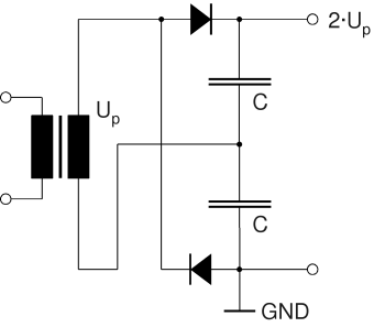 |
Alternative Full-Wave Doubler
With this circuit, I found a Zi/XC value of approx. 3.6. Compare this with the doubler circuits shown above!
Will be continued...