High Voltage and X-Ray Experiments
Text and Graphics Copyright © 2005 − 2008 Henning Umland
The following descriptions are given for the purpose of information only. I do not encourage ANYBODY to conduct experiments like those shown below, and I do not assume liability for any damage resulting from such experiments. People working with high voltage and X-rays should have a solid background in physics and electronics and should know what they are doing. The high voltage sources described here are much more powerful than generators of static electricity like, e. g., influence machines, Van de Graaff generators, etc. High voltage can kill instantly, X-rays in the long run (radiation sickness, cancer) if not handled properly.
Experiments with Various Multiplier Designs (II)
In the preceding chapter, the output impedance of various multipliers as a function of stage capacity, frequency, stage number, phase number, and other design characteristics was determined experimentally. This chapter gives an account of the lab trials I made in order to learn more about the behavior of a multiplier circuit running under load and particularly about the voltage and current distribution inside the circuit.
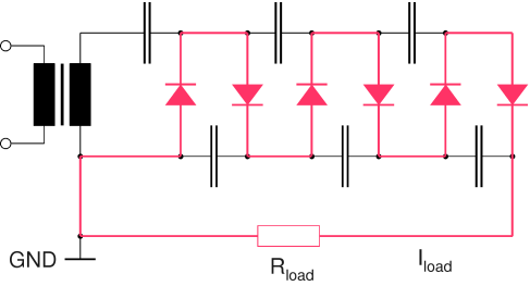
The first thing I learned is that in ANY multiplier running under load the average DC current flowing through each diode, Idiode, is the same. This can be checked easily by connecting a current meter in series with any chosen diode in the circuit. Since the capacitors in a multiplier circuit block any DC current, the latter has to flow through the diodes. Since the diodes are connected in series, each diode bears the same DC current. This is illustrated by the following circuit diagram. The path of the DC current is drawn in red:
|
Path of DC Current in Half-Wave Multiplier
The diode current in a full-wave multiplier is half the DC load current since the latter is divided between two diode stacks. Accordingly, the diode current in a 3-phase multiplier is one third of the load current:
Idiode = Iload / number of phases
In a half-wave multiplier with an odd multiplication factor, e. g., a tripler, the full DC current flows through the secondary coil of the transformer (see below). Under heavy load, this may lead to core saturation, resulting in a high magnetizing current and increased transformer losses.
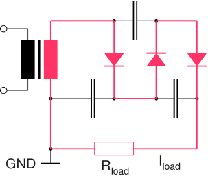 |
Path of DC Current in Half-Wave Tripler
In a full-wave multiplier fed by a single transformer with a center-tapped secondary coil this problem does not occur, because the magnetic fields generated by the DC currents flowing through the secondary coil cancel each other.
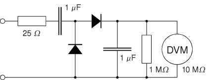
For the following measurements, I built two voltage probes. The first one, consisting of a low-pass filter and a DVM, is used to measure the average DC voltage across a capacitor, suppressing the ripple voltage. The other one, consisting of a voltage doubler and a DVM, is used to measure the ripple voltage (peak to peak) dropping across a capacitor without the DC component. The forward voltage of the Si-diodes (approx. 0.7 V) was ignored during the measurements.
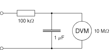
DC Voltage Probe
Peak-to-Peak Voltage Probe
The experiments were made with full-wave circuits because these proved to be most suitable for my HV experiments and had the highest priority. Half-wave circuits may follow later. Again, the secondary voltage of each transformer is approx. 43 V RMS.
Three-stage multiplier:
The first circuit I studied was a full-wave multiplier with three doubler stages, as shown in the following diagram:
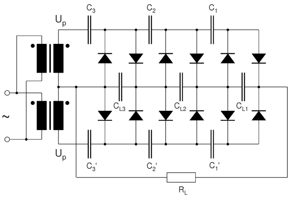 |
Full-Wave multiplier with 3 Doubler Stages
Under no-load conditions, all capacitors except C3 and C3' (the charging capacitors connected to the transformer) would be charged up to 2√2·URMS. The DC voltage across C3 and C3' would be √2·URMS each (neglecting the forward voltage of the diodes). No ripple voltage would be detected across any capacitor in the circuit. The following table shows the average DC voltage, UDC, and the peak to peak ripple voltage (UP-P) measured accross each capacitor when the multiplier is connected to a 3.05 kΩ load resistor:
RL = 3.05 kΩ
C [µF]
UDC [V]
UP-P [V]
C1, C1'
40
47.3
13.6
C2, C2'
40
65.3
28.2
C3, C3'
40
39.7
42.5
CL1
40
40.7
6.7
CL2
40
51.4
5.1
CL3
40
77.5
5.3
The DC voltage dropping across RL is 169.5 V under these conditions (no-load output voltage = 353.5 V). Within the experimental error, the DC output voltage is the sum of the DC voltages dropping accross the three load capacitors (CL1 thru CL3). By contrast, the ripple voltage measured across RL (UP-P = 14.0 V) is significantly smaller than the sum of the ripple voltages measured across each load capacitor (17.1 V). This is a clear indication that these AC voltages are not exactly in phase! It seems that the ripple voltage across each load capacitor undergoes a phase shift from stage to stage. If this is the case, it should be possible to find conditions (load current, stage number) where the ripple voltage across RL becomes very small or even zero. We will see that later.
The circuit further exhibits a change of the AC voltage (peak to peak, Up-p) dropping across the charging capacitors. The ripple voltage across the charging capacitors of the stage connected to the load resistor (C1 and C1') is smallest. The ripple voltage increases from stage to stage and is highest at the stage connected to the transformer. The ratio of the ripple voltages thus measured is approximately 1:2:3. This should also apply to the AC currents flowing through these capacitors. Thus, the charging capacitors near the transformer are subjected to more dielectric losses than the others and should have the highest probability of premature failure. It is therefore desirable to "equalize" the stress acting on the capacitors. For the next experiment, the charging capacitors match the current distribution, i. e., the ratio of their capacitances is also 1:2:3:
RL = 3.05 kΩ
C [µF]
UDC [V]
UP-P [V]
C1, C1'
20
48.6
30.6
C2, C2'
40
77.7
30.8
C3, C3'
60
46.6
30.7
CL1
40
34.8
7.6
CL2
40
61.6
5.6
CL3
40
91.4
5.4
As expected, the ripple voltages across the charging capacitors are equal now. Besides that, the load current rises from 55.7 mA to 61.2 mA, i. e., by approx. 10%. Thus, we have not only improved the reliability of the circuit but also the efficiency without using additional capacitance! The ripple voltage across the load resistor remains virtually unchanged (14.2 V vs. 14.0 V).
As with the preceding circuit, the ripple voltage across CL1' is comparatively high. Although this is not dramatic, I tried to equalize the ripple voltages dropping accross the load capacitors as well. For this purpose, I increased CL1 to 60 µF:
RL = 3.05 kΩ
C [µF]
UDC [V]
UP-P [V]
C1, C1'
20
48.1
30.3
C2, C2'
40
77.5
30.5
C3, C3'
60
46.4
30.4
CL1
60
34.5
5.3
CL2
40
61.1
5.5
CL3
40
90.9
5.3
The table confirms that the ripple voltages are almost equal now. The load current remains almost unchanged (61.1 mA) but the ripple voltage across RL is reduced from 14.2 V to 12.9 V (at this particular load current!).
In all three circuits the DC voltages across the load capacitors decrease in the order CL3 → CL2 → CL1. This change is less pronounced in the first circuit (the one with equal charging capacitors).
Four-stage multiplier:
After these initial trials I built a full-wave multiplier with four doubler stages, as shown in the next circuit diagram. Since this is a model for my 160 kV multiplier, I wanted to study it more thoroughly. I did not pursue the design with equal charging capacitors any further because the preceding experiments clearly showed that it is comparatively inefficient.
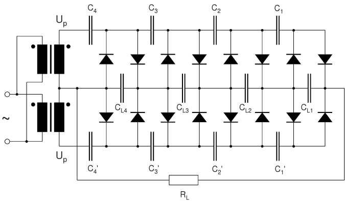 |
Full-Wave Multiplier with 4 Doubler Stages
The photo shows the experimental setup of the multiplier (the grey box in the background is a shortwave receiver and has nothing to do with the circuit):
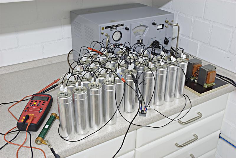 |
Experimental Setup of 4-Stage Multiplier (Number of 20 µF Capacitors: 28 )
For the first experiment of this series, I chose 40 µF (= 2×20µF) load capacitors (CL1 thru CL4). Again, RL was 3.05 kΩ. The following results were obtained:
RL = 3.05 kΩ
C [µF]
UDC [V]
UP-P [V]
C1, C1'
20
17.0
30.1
C2, C2'
40
45.4
30.3
C3, C3'
60
75.3
30.1
C4, C4'
80
44.9
29.9
CL1
40
4.3
5.4
CL2
40
30.6
4.7
CL3
40
59.7
4.3
CL4
40
89.6
4.8
The no-load ouput voltage was 466 V. The DC voltage dropping across RL was 184 V. The ripple voltage (UP-P) across RL was 4.9 V. The latter is much smaller than the sum of the ripple voltages dropping across the load capacitors CL1, CL2, CL3, and CL4, respectively (∑ = 13.8 V). As with the three-stage multiplier, the ripple voltage across CL1 is highest. To decrease it, I increased CL1 to 50 µF:
RL = 3.05 kΩ
C [µF]
UDC [V]
UP-P [V]
C1, C1'
20
16.9
30.0
C2, C2'
40
45.0
30.2
C3, C3'
60
74.7
30.1
C4, C4'
80
44.5
29.9
CL1
50
4.4
4.4
CL2
40
30.4
4.7
CL3
40
59.2
4.3
CL4
40
88.8
4.8
The result appeared successful at first glance, but the ripple voltage across RL increased by about 10% (from 4.9 V to 5.4 V). This may depend on the load current, however.
For the next experiment, I reduced each load capacitor to 20 µF:
RL = 3.05 kΩ
C [µF]
UDC [V]
UP-P [V]
C1, C1'
20
18.2
30.6
C2, C2'
40
45.2
30.8
C3, C3'
60
75.1
30.6
C4, C4'
80
44.9
30.2
CL1
20
6.8
8.7
CL2
20
30.6
6.5
CL3
20
59.3
5.3
CL4
20
89.0
6.4
As expected, the ripple voltages across the load capacitors are higher now. The ripple voltage across RL increased from 4.9 VP-P to 5.4 VP-P (not as much as expected). The DC output voltage, however, remains virtually constant (186 V), i. e., the output impedance is independent of the load capacitors!
The next table shows the results obtained with the same capacitors but reduced load current (RL = 6.1 kΩ):
RL = 6.1 kΩ
C [µF]
UDC [V]
UP-P [V]
C1, C1'
20
47.7
21.7
C2, C2'
40
66.3
21.9
C3, C3'
60
86.9
21.8
C4, C4'
80
48.5
21.7
CL1
20
38.8
9.0
CL2
20
55.4
6.0
CL3
20
75.4
4.8
CL4
20
95.5
4.3
Under these conditions, the output voltage is 266 V (466 V no-load voltage). As expected, the DC voltage across each capacitor is higher than before. With the exception of CL1, the same applies to the AC voltage. The surprise came when I measured the ripple voltage across RL. In spite of the lighter load, it has risen to 20 VP-P!
Again, I increased CL1 in order to reduce the ripple voltage dropping across this capacitor:
RL = 3.05 kΩ
C [µF]
UDC [V]
UP-P [V]
C1, C1'
20
17.7
30.2
C2, C2'
40
45.0
30.5
C3, C3'
60
74.7
30.2
C4, C4'
80
44.8
30.0
CL1
30
6.0
6.4
CL2
20
30.6
6.3
CL3
20
59.1
5.2
CL4
20
88.6
6.3
As expected, the ripple voltage across CL1 decreased. The output ripple voltage, however, went up again (from 5.4 V to 5.9 V). Therefore, I abandoned this design and chose equal load capacitors for my further experiments.
From the experimental results obtained up to now, we can draw the following conclusions for the design of full-wave multipliers:
The somewhat confusing results regarding the ripple voltage made it necessary to explore the output voltage (DC and AC component) over a wider range of load currents.
The first experiment was made with 20 µF load capacitors. First, the average DC output voltage at various load currents was measured. The diagram shows the DC output voltage as a function of the load current (data points and a smoothed U/I curve obtained with the B-spline method):
.png) |
DC Output Voltage vs. Load Current (load capacitor: 20 µF / stage)
The curve indicates that there is a fairly linear U/I relationship at low load currents. The curve flattens out only after the output voltage has dropped below approx. 40% of the no-load voltage.
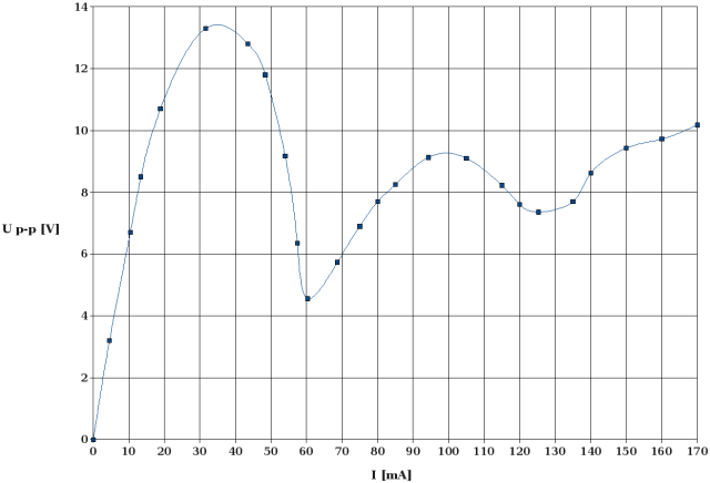
The next diagram shows the ripple voltage, UP-P, as a function of the DC load current:
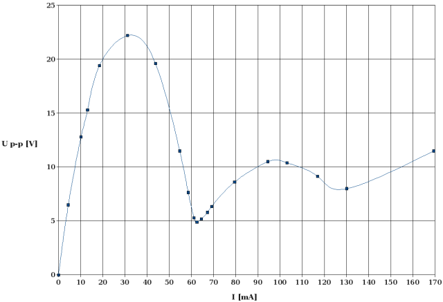 |
Ripple Voltage (Peak to Peak) vs. Load Current (load capacitor: 20 µF / stage)
The result is quite surprising. Initially, the ripple voltage rises in proportion with the load current, as expected. Then, however, the curve flattens out, and the ripple voltage passes through a broad maximum followed by a sharp minimum. Another maximum followed by a less distinct minimum occurs as the load current increases further. How do we explain this strange behavior? Presently, only one explanation comes to my mind: As soon as a load current occurs, a ripple voltage drops across each capacitor of the the load stack. At low load currents, the ripple voltages are almost in phase, and the ripple voltage at the load resistor is almost the sum of the ripple voltages measured across the respective load capacitors. As the load current increases, there is a growing phase shift of the ripple voltage from stage to stage, and the voltage measured across the load resistor becomes smaller than the sum. Finally, when the pase angle becomes high enough, ripple voltages of certain stages cancel each other (not totally since the amplitudes are different). This is when the curve passes through a minimum.
These are probably rather exotic operating conditions for a multiplier. Under heavy load, a multiplier with a lower number of stages would be more efficient in many cases since the voltage drop would be much smaller.
I repeated this experiment with 40 µF load capacitors. The respective curves for DC voltage and ripple voltage vs. load current are shown below.
.png) |
DC Output Voltage vs. Load Current (load capacitor: 40 µF / stage)
The above DC curve looks like an almost perfect copy of the one obtained with 20 µF load capacitors. This again confirms that the DC voltage drop under load is independent of the chosen load capacitors (probably within certain limits).
 |
Ripple Voltage vs. Load Current (load capacitor: 40 µF / stage)
The ripple voltage curve shows the same pattern as the one with the 20 µF capacitors. As expected, the ripple voltage at a given load current is lower when bigger load capacitors are chosen since these store more energy and smooth the output voltage more efficiently than smaller capacitors. Interestingly, the ripple voltage does not decrease as much as expected when increasing the load capacitance from 20 µF to 40 µF per stage.
Will be continued...